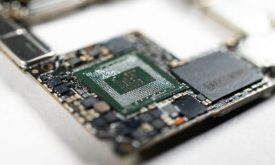
Semiconductor
TSMC opened new R&D center for 2nm, 1.4nm and smaller chipset research

A few days ago, the world’s largest semiconductor producer – Taiwan Semiconductor Manufacturing Co (TSMC) inaugurated a brand new global R&D center in Hsinchu, Taiwan.
The aim of this research and development facility is to harness chipset processing technology of 2nm and beyond. According to the information, the new TSMC R&D center initially hosted 2000 engineers and this capacity is aimed to increase to 7000 by September.
TSMC chairman Mark Liu said that the company is focused on advanced chip technologies and will be more proactive in developing world-leading semiconductor technologies from 2-nanometer technology.
The company also projects that 2nm tech would be popular by 2025 and follow the success of 3nm in the industry. TSMC is also counting Apple and Nvidia as its major customers.
Talking about investment, TSMC is continuously increasing its R&D fund. Last year, TSMC spent 30 percent more on R&D, totaling US$5.47 billion, compared with US$4.47 billion in 2021.
Overseas development:
Amid this grand opening, TSMC keeps on expanding its chipset manufacturing plant in overseas markets. Recently, the chip maker announced a 28nm plant in Germany. However, this move sparked some questions over TSMC the company will halt in-house manufacturing. But the chip manufacturer now denied all of these allegations with this new R&D facility.