News
New Huawei chipset packaging could reduce manufacturing cost
Recently, the Chinese Patent Department published a new Huawei patent on a chipset packaging technology that could reduce the overall manufacturing cost of the semiconductor. This is a new addition to patents, which appeared in line with Huawei’s chipset manufacturing research.
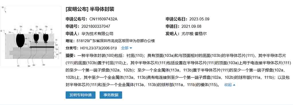
According to the information, Huawei filed this patent with application number CN116097432A, which is titled “semiconductor packaging”. This patent was applied on September 8, 2021, and published (accepted) on May 9th, 2023.
Technical details:
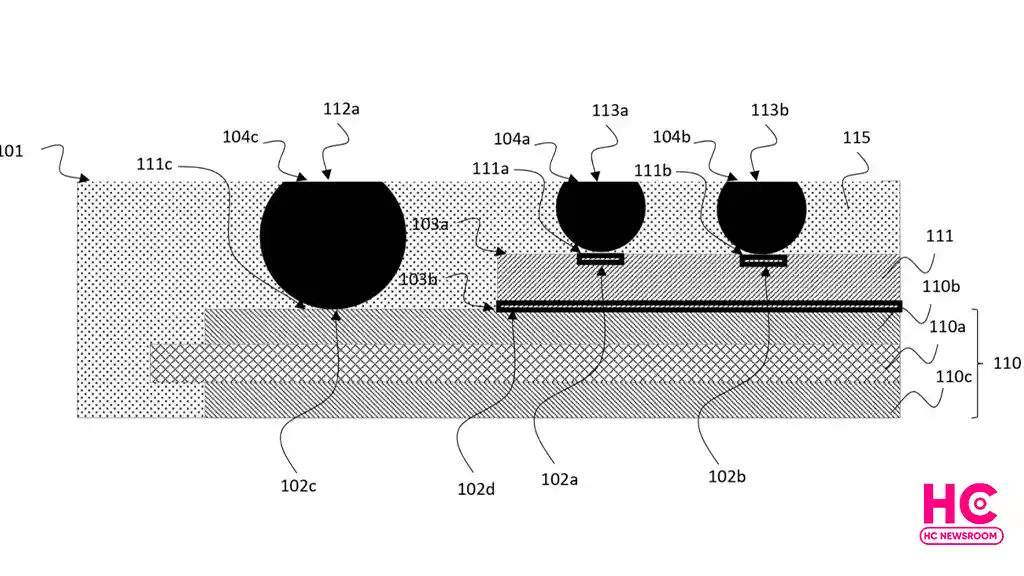
It includes a semiconductor package (100) with a substrate (110), a semiconductor chip (111) having a top surface (103a) and a bottom surface (103b) opposite to the top surface, wherein the bottom surface of the semiconductor chip (111) (103b) placed on the substrate (110).
Inside the semiconductor chip (111) includes at least one first terminal pad disposed on the top surface (103a) of the semiconductor chip (111) for electrically connecting the semiconductor chip (111) (102a, 102b).
At least one all-metal body (113a, 113b) is placed on at least one first terminal pad (102a, 102b) of the semiconductor chip (111), wherein at least one all-metal body (113a, 113b) has a spherical portion (111a, 111b) electrically connected to at least one first terminal pad (102a, 102b).
There is a spherical portion (111a, 111b) enclosing a semiconductor chip (111) and at least one full metal body (113a, 113b) ) motif (115).
Cost-effective:
It is said that this tech could provide an alternative mold embedding solution and reduces the cost of manufacturing. It also provides efficient and reliable manufacturing of semiconductor packages.
What is Semiconductor packaging?
A semiconductor package is a metal, plastic, glass, or ceramic casing containing one or more semiconductor devices or integrated circuits. Individual components are fabricated on semiconductor wafers (commonly silicon) before being diced into the die, tested, and packaged. The package provides a way for connecting it to the external environment, such as a printed circuit board, using leads such as lands, balls, or pins.
It provides protection against threats such as mechanical impact, chemical contamination, and light exposure. Additionally, it helps dissipate heat produced by the device, with or without the aid of a heat spreader.
Continue to explore:
This new chipset packaging technology patent from Huawei reveals the company’s continues efforts in order to achieve effective semiconductor manufacturing.
(via)