Technology
Huawei patents chip and its production method technologies
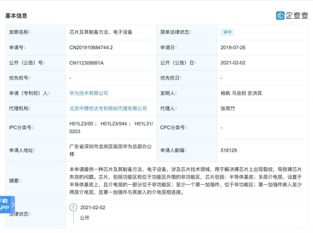
On July 27, 2019, Huawei has filed a new patent for the chip and its preparation method, which is passed and publically published on February 2 with publication number CN112309991A in China.
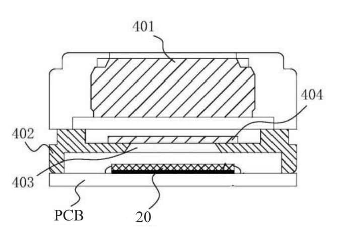
The patent describes that this application provides a chip and its preparation method and electronic equipment, which relates to the field of chip technology. This method is used to solve the problem that cracks appear on the bare chip and cause the failure of the bare chip.
The bare chip architecture includes a multilayer dielectric layer arranged on the semiconductor substrate, a part of the dielectric layer is placed on the non-functional area and at least one first reinforcement located in the non-functional area. The first reinforcing member is embedded in at least two dielectric layers, and the first reinforcing member is connected to the embedded dielectric layer.
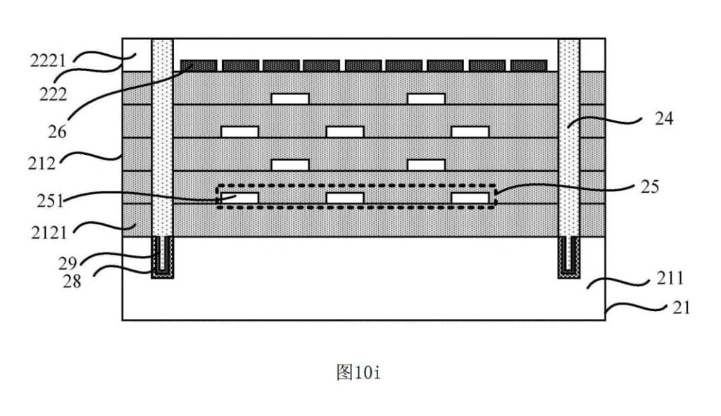
The core component of the electronic system is the bare chip and the structure of the chip determines the stability of the system. When the bare chip is manufactured and packed, it is very common to crack occurs between the dielectric layers. After being heated and pressed, the layers are either broken or cause a failure problem.
To get rid of this problem, the non-functional area has the first reinforcement that will extend and block the cracks. Simultaneously the thermal stress can be reduced by 30%, which also lowers down the probability of cracks and improves the chip strength.
[Via]